§ 2.14 - Test Points
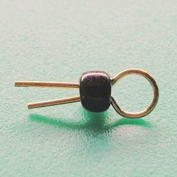
Back to → Main Power Block PageThe Power Block PCB provides for 12 optional test points; you can obtain the correct test point components from the link on the Power Block Parts Sources page. When installed, they enable easier connection of lab analysis equipment — spectrum analyzer, DVM, oscilloscope, etc. You may find them useful.
For each test point:
- Insert the slightly longer lead into the test point's via (PCB through hole), which is very small (intentionally so, otherwise the test points fall out.)
- While holding the test point down from the top, push the test point's bead down to the surface of the PCB, which pinches the shorter wire against the longer wire.
- Wiggle the test point just a little bit and both leads will slip through the PCB via, and because the fit is tight and the leads naturally spring away from each other, the test point will stay put until you're ready to solder it. You can solder after each insertion, or after they're all inserted. Check the loop alignment before you solder.
Solder and trim the test point leads on the solder side of the PCB.
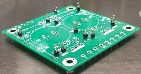
§ 2.14.1 - Test Point Function
All test points are measured against / referenced to ground (TP11 or TP12), and these designations refer to the PCB silkscreen designations, which in turn are for a plus & minus build. If you build a minus & minus Power Block, or a plus & plus Power Block, then the output voltages and/or waveforms to be expected at the test points change accordingly, but the PCB designations as listed here remain the same:
- 78XX output voltage (+)
- 79XX output voltage (-)
- -- supply battery backup input voltage
- 79XX output voltage (-)
- ++ supply battery backup voltage
- 78XX output voltage (+)
- ++ unregulated supply voltage
- -- unregulated supply voltage
- AC1 input from T1
- AC2 input from T1
- Ground
- Ground
, Previous Page . Next Page
o Ordering g Glossary s Sitemap u Updates
![]()